CMPL SEMICON
National Institute of Physics
University of the Philippines - Diliman
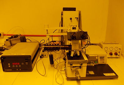
The laboratory uses various techniques in device fabrication such as photolithography, metallization and chemical etching. The lab houses a Karl Suss Mask Aligner which aids the use of a photomask to selectively expose a selected pattern onto a sample coated with a polymer. Resistive evaporation usually follows this process in order to deposit a thin film of metal onto the sample that could serve as a contact for a device.
Photolithography
Photolithography is a patterning technique which utilizes a photoresist, a mask and UV source to pattern the shape of the desired contact onto a substrate. The resolution of a pattern can be minimized up to as small as 2 microns, even smaller than the diameter of a human hair. The mask's pattern is transferred onto the substrate through the reaction of the photoresist with the UV source. The process is followed by developing the photoresist from the sample for metal deposition of the device contacts. To complete the lithography is then completed by removing the excess photoresist to reveal the patterned metal. The CMPL-Semicon group uses a Karl-Suss MJB-3 mask aligner acquired in 2000 through a DOST-PCASTRD grant.

Metallization
Metals are usually deposited onto patterned samples using thermal evaporation. At high enough temperatures, the evaporation and condensation of a metal can be utilized in order to form a thin film of that metal that would serve as a contact of semiconductor devices. This can be done by using (1) resistive evaporation, which involves passing a high current through a filament to melt then evaporate a metal or (2) Electron beam evaporation which involves heating the metal directly by using a focused beam of high energy electrons.