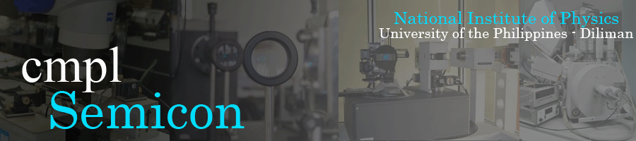
CMPL SEMICON
National Institute of Physics
University of the Philippines - Diliman
FACILITIES


DEVICE FABRICATION
The laboratory uses various techniques in device fabrication such as photolithography, metallization and chemical etching. The lab houses a Karl Suss Mask Aligner which aids the use of a photomask to selectively expose a selected pattern onto a sample coated with a polymer. Resistive evaporation usually follows this process in order to deposit a thin film of metal onto the sample that could serve as a contact for a device.
CHARACTERIZATION
The laboratory has a variety of optical characterization tools to asses the quality and performance of the samples and devices fabricated in the lab. Techniques such as transmission and reflection spectroscopy, together with photocurrent and photoreflectance are some of the experiments used in characterizing thin films and various heterostructures
GROWTH
The CMPL-Semiconductors Group practices different growth techniques using the RF Magnetron Sputtering System and Molecular Beam Epitaxy (MBE). These facilities are used for growth of thin films and several nanostructures that could be used in different devices.